- 您现在的位置:买卖IC网 > Sheet目录2007 > LTC6991MPS6#TRPBF (Linear Technology)IC OSCILLATOR RESET LF TSOT23-6
LTC6991
18
6991fb
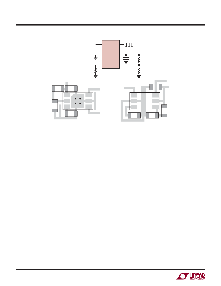
1. Connect the bypass capacitor, C1, directly to the V+ and
GND pins using a low inductance path. The connection
from C1 to the V+ pin is easily done directly on the top
layer. For the DFN package, C1’s connection to GND is
also simply done on the top layer. For the TSOT-23, OUT
can be routed through the C1 pads to allow a good C1
GND connection. If the PCB design rules do not allow
that, C1’s GND connection can be accomplished through
multiple vias to the ground plane. Multiple vias for both
the GND pin connection to the ground plane and the
C1 connection to the ground plane are recommended
to minimize the inductance. Capacitor C1 should be a
0.1μF ceramic capacitor.
2. Place all passive components on the top side of the
board. This minimizes trace inductance.
3. Place RSET as close as possible to the SET pin and
make a direct, short connection. The SET pin is a
current summing node and currents injected into this
pin directly modulate the operating frequency. Having
a short connection minimizes the exposure to signal
pickup.
4. Connect RSET directly to the GND pin. Using a long path
or vias to the ground plane will not have a significant
affect on accuracy, but a direct, short connection is
recommended and easy to apply.
5. Use a ground trace to shield the SET pin. This provides
another layer of protection from radiated signals.
6. Place R1 and R2 close to the DIV pin. A direct, short
connection to the DIV pin minimizes the external signal
coupling.
6991 F18
LTC6991
RST
GND
SET
OUT
V+
DIV
C1
0.1μF
R1
R2
RSET
V+
DIV
SET
OUT
GND
RST
C1
R1
R2
V+
RSET
DFN PACKAGE
RST
GND
SET
OUT
V+
DIV
R2
V+
RSET
TSOT-23 PACKAGE
R1
C1
Figure 18. Supply Bypassing and PCB Layout
APPLICATIONS INFORMATION
发布紧急采购,3分钟左右您将得到回复。
相关PDF资料
LTC6992MPS6-4#TRPBF
IC OSC PWM VOLT CTLR TSOT23-6
LTC6994CDCB-2#TRPBF
IC DELAY LINE 6-DFN
LTC7541ABN#PBF
IC CMOS D/A CONV 12BIT 18-DIP
LTC7545ACG#TRPBF
IC D/ACONV MULTIPLY 12BIT 20SSOP
LTC8043EN8
IC D/A CONV 12BIT SERIAL 8-DIP
LTC8143ESW#TRPBF
IC D/A CONV 12BIT SERIAL 16-SOIC
LTM9011CY-14#PBF
IC ADC 14BIT UMODULE 140BGA
LV5609LP-E
IC CLOCK DRIVER VERTICAL 24VCT
相关代理商/技术参数
LTC6992-1
制造商:LINER 制造商全称:Linear Technology 功能描述:TimerBlox Voltage-Controlled Pulse Width Modulator (PWM)
LTC6992-2
制造商:LINER 制造商全称:Linear Technology 功能描述:TimerBlox Voltage-Controlled Pulse Width Modulator (PWM)
LTC6992-3
制造商:LINER 制造商全称:Linear Technology 功能描述:TimerBlox Voltage-Controlled Pulse Width Modulator (PWM)
LTC6992-4
制造商:LINER 制造商全称:Linear Technology 功能描述:TimerBlox Voltage-Controlled Pulse Width Modulator (PWM)
LTC6992CDCB-1#PBF
制造商:Linear Technology 功能描述:SC-Timing, Cut Tape PWM with 0% to 100% Pulse Width Control
LTC6992CDCB-1#TRMPBF
功能描述:IC OSC SILICON 1MHZ 6-DFN RoHS:是 类别:集成电路 (IC) >> 时钟/计时 - 可编程计时器和振荡器 系列:TimerBlox® 标准包装:3,000 系列:- 类型:振荡器 - 晶体 计数:- 频率:- 电源电压:2.3 V ~ 5.5 V 电流 - 电源:1.07mA 工作温度:-30°C ~ 80°C 封装/外壳:SOT-665 包装:带卷 (TR) 供应商设备封装:SS迷你型-5D 安装类型:表面贴装 其它名称:AN8955SSMTXLTR
LTC6992CDCB-1#TRPBF
功能描述:IC OSC SILICON 1MHZ 6-DFN RoHS:是 类别:集成电路 (IC) >> 时钟/计时 - 可编程计时器和振荡器 系列:TimerBlox® 产品培训模块:Lead (SnPb) Finish for COTS
Obsolescence Mitigation Program 标准包装:45 系列:- 类型:温度 - 补偿晶体振荡器(TCXO) 计数:- 频率:25MHz 电源电压:3.135 V ~ 3.465 V 电流 - 电源:1.5mA 工作温度:-40°C ~ 85°C 封装/外壳:16-SOIC(0.295",7.50mm 宽) 包装:管件 供应商设备封装:16-SOIC W 安装类型:表面贴装
LTC6992CDCB-1TRMPBF
制造商:Linear Technology 功能描述:PWM Voltage Controlled 3.81Hz-1MHz DFN6